
This series will discuss the basic building blocks of a simple theoretical CPU design. In it, I’ll cover one topic in each article and append the theoretical design. In the end, we’ll have a functioning CPU model.
I’m planning to make this a larger series of articles and videos about how to build your completely custom computer from scratch. I also plan to write an OS for the machine later.
How to design your own CPU from scratch (4 parts)
Here I plan to design a really simple 8-Bit CPU from scratch, only using low-level logic and low-level components. I’ll also discuss the main parts of a CPU and maybe I’ll discuss extended features and pipelining at the end of the series or in a future article.
How to build a custom computer from scratch (5 parts)
Here I plan to build everything around the CPU that’s needed. In this series, I’ll design my own mainboard with I/O and a simple graphics chip that outputs VGA. I’ll talk about all the important topics in their respective articles of this series.
How to design and code a custom operating system
This is something that I plan to do in the future and it’s something that I wanted to try since I first started programming.
What does a CPU consist of?
That’s not that easy to answer, especially if you look at modern-day CPUs that have so many different features that one could write a series of books about them. However I want to focus on the most simple (yet somewhat practical) CPU design, I can think of: An 8-Bit CPU without pipelining and without any extended features. It’s going to be pretty inefficient, but it should be easy to understand. I want to keep it as simple as possible, so that everybody (that’s interested in the topic) can understand the core concepts.
The ALU
This is the part in a CPU that takes care of calculations. The acronym stands for “Arithmetic-Logic-Unit”. It is an electronic circuit that combines different arithmetic and bitwise logic operations. The very basic functionality, that each ALU has to have (otherwise it wouldn’t make any sense), is the arithmetic addition and the logic-functions AND and NOT or OR and NOT, as they are complete, which means that you can derive every other logic function by using these two. By the way, the combined functions (NAND and NOR) and complete as well.
Data/Instruction memory
There needs to be some way to store results from previous calculations. In a microprocessor, this usually happens in registers. (For an example see this article, to be more precise: the PRU program portion). In our case, one word consists of 8-Bits and one register in this CPU can store 8-Bit.
However, registers are not meant to store data permanently. They are only used for storing results from previous calculations to use them in future calculations. To store values for a longer time, RAM is the way to go. To store them permanently, even after powering the system off, other methods, like hard-disk-drives, are used.
In my design, the data and instructions are stored separately. This architecture is known as the “Harvard architecture“. Combined storage of instructions and data in one storage is also referred to as the “Von-Neumann architecture“.
I plan to use 16 registers, from which only 13 can be used by the application programmer. The three registers, that are read-only, will hold the values for -1, 0 and 1, so in binary (1111 1111), (0000 0000) and (0000 0001), to make it easy to in- and decrement values and to delete a stored value.
If you look at all the registers of the CPU, the resulting table is often referred to as the “register-file“. Sometimes, it’s also called “scratchpad”.
Shifter
A shifter is usually also included in a CPU. The simplest possible shifter allows the programmer to shift the result of the last calculation by 1-bit either to the left or to the right. It’s also possible not to shift at all. More advanced CPUs allow the programmer to shift multiple positions or to rotate binary values.
My CPU will only allow the user to shift the result by one position (left or right) or not shift at all.
A clock
Obviously, the complete circuit will need to have a signal that tells all the individual components and sections when they should do their work. As this CPU will won’t have any pipelining, we’ll need to delay the clock for each individual section so they’ll know when to work.
If you use pipelining, the sections you usually have are: Instruction fetch, instruction decode (register values are obtained here), execute, store and write-back. We’ll need similar sections that I’ll discuss in more detail later.
Busses
We’ll have to load and store bits during our calculations, so we’ll need some lines where the information can travel. These coherent lines are called a bus. We could either load all bits simultaneously (parallel) or one bit after another (serial).
The main busses will be between the register-file and the ALU, the ALU and the program-memory and the whole CPU and an external memory (or memory controller to be more precise), for storing data in RAM or persistent memory.
Summary
For a CPU to make sense, it has to consists of a unit that calculates values, data storage and busses that connect the components and transfer data. Everything is controlled by a clock signal.
Like I said above, this is by no means a complete list. These are the very basic components of the CPU I want to design. I linked further resources at the relevant positions. I’ll also explain the parts in more detail when I show you the individual designs.
The ALU in more detail
Like I stated above, this part is responsible for all the calculations. Usually, the ALU is symbolized by a v-shape with the in- and output-lines:

A and B are the data words that are going to be used in the next calculation. F represents the input flags which are used for several things. For example, it lets the ALU know what the next instruction is and how to calculate the result (R).
The output-flags (D) can be used by the application programmer. The ALU might have a line that gets high, when the last result was 0, or when it was negative. There might be more flags present and I’ll use these for jumps in applications in my CPU.
Arithmetic functions in the ALU
In this section, I’ll only look at different types of binary addition circuits, because that’s the only function my ALU will support as all the other simple arithmetic operations can be derived from the addition.
One-Bit-Addition
I’ll start with the simplest of all possibilities. Just imagine that you only have two one-bit words you want to calculate. The output also consists of one bit.
Half-adder
The half-adder adds two one-bit binary digits without considering a previous carry, that might have occurred during a previous addition. So it has two inputs: A and B and two outputs: S and C which stand for sum and carry.
The following table illustrates what the results of this adder look like:
| A | B | S | C |
| 0 | 0 | 0 | 0 |
| 0 | 1 | 1 | 0 |
| 1 | 0 | 1 | 0 |
| 1 | 1 | 0 | 1 |
nThis adder can be built by using an XOR and an AND gate and it looks like this:

Try it here: https://simulator.io/board/EQtBqeqqlX/1
Full-adder
The full-adder is very similar to the half-adder from above. The only difference is, that it has an additional input, often named Cn-1 or Ci, which stands for a carry-in-bit from a previous addition.
The full-adder logic looks like this:

Try it here: https://simulator.io/board/yWjR39XAbl/1
n-Bit addition
As stated above, this CPU will operate on 8-Bit long data words. Therefore the ALU will have to be able to add two 8-Bit numbers. So we’ll have to combine the 1-Bit adders from above to form a larger network. There are some popular methods but I only want to discuss two of them:
Carry-ripple adder
I will start with the easiest to understand. The first stage can be a full-adder but I’ll use a half-adder because my CPU will simply ignore if there was a carry-out in the last addition. The rest of the carry-ripple-adder is made up of full-adders.
The inputs A and B are the respective bits you want to add and the carry-in of one adder is connected to the carry-out of the previous one. The last FA’s carry-out is the carry-out of the whole 8-Bit carry-ripple-adder.
So let’s take a look at a 4-Bit carry-ripple-adder (of course the 8-Bit one would have 16 inputs and 8 adders in total, but this is enough to show the functionality):
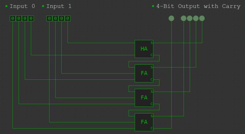
Try it here: https://simulator.io/board/JIxRlrtGhm/1 (pre-made example)
A good thing about this circuit is that it’s simple to build and easy to understand. The relatively slow calculation is one negative side effect.
By the way, I built this adder in LBP a while ago. Here’s a quick demo of how full-adders and the carry-ripple adder work:
Carry-lookahead adder
This circuit is much more complex and therefore harder to think through. However, it’s quicker and it looks like this:

The idea behind this method is that you don’t have to wait for the results to pass through all the adders before you can calculate your final result.
In the carry-lookahead adder, we determine whether a bit is being carried out or not after a specific position and then we can calculate different parts of the numbers at once. For example, if there are two 4-Bit numbers put into the adder we determine whether the last two bits will generate a carry-out and then use this information to calculate the sum of the first two bits simultaneously with the sum of the last two bits and then output the complete resulting 4-Bit word. That’s why this adder is also sometimes referred to as a ‘parallel-adder’ or ‘PA with lookahead’.
A really good and more detailed explanation can be found in this article.
Block diagram
The following block diagram explains the ALU and the in- and outputs. I decided to go with the carry-ripple adder, simply because it’s easy to implement and build and I don’t care about performance too much in this case.
However, here’s the ALU in all its glory:
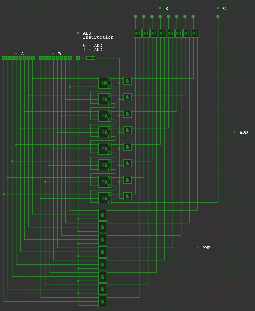
Try it here: https://simulator.io/board/QjuAxAT5Ua/2
In the next part…
… I want to talk about how the ALU is controlled, where data is stored and how it is transferred into the ALU and back to the memory.
Table of contents
Part 1 – Basics and the ALU (You are here)
Part 2 – Registers and memory
Part 3 – Applications
Part 4 – The completed CPU
Additional resources
Adders, Wikipedia
Online logic editor and simulator, simulator.io
Image sources
[Fig. 1] An ALU, Wikipedia
[Fig. 5] CLA, Wikipedia


What is the purpose of the final OR gates (the ones fed by the outputs of the AND and ADD outputs) before the result output?
LikeLike
Thanks for the cpu articles! I really need your articles on building a computer and os.
LikeLike
Thanks, I’m glad you like them!
I started working on the computer article some time ago, but I think that’ll need some more time before it’s done. Unfortunately, I haven’t even started working on a custom operating system yet. However, maybe you’ll find this document useful: https://www.cs.bham.ac.uk/~exr/lectures/opsys/10_11/lectures/os-dev.pdf
LikeLike
Thanks for the answer and the link. I will wait for your articles 🙂
LikeLike
Really cool! Fascinating how I always thought how complex a cpu has to be and then you break it down to such a simple level. Well done! Also really cool that you included that little video. I personally dont play this game but nice that you made that effort of showing us the principles in a playful way
LikeLiked by 1 person
Thanks a lot, I’m glad you liked it! Yeah, but keep in mind, that this design is very very simple and inefficient. The whole point of it was to understand the basic principles. If you look at a real CPU, you’ll find the described parts in it, but it will have a lot more features and it will look a lot more complicated.
LikeLike